Bulk metallic glasses

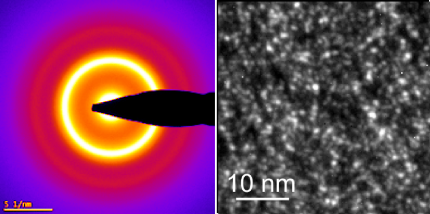
Color coded diffraction pattern and TEM dark-field image of amorphous CuZr.
Copyright C. Rentenberger
Bulk metallic glasses
Bulk metallic glasses are a relatively new kind of materials with very interesting properties (e.g. exceptional strength and an impressive elastic limit). The properties are associated with the strong tendency to vitrification upon cooling leading to an amorphous structure without long-range atomic order. Still, some ordering on short-range (up to 0.5 nm) and medium-range (up to 2 nm) scales is present.
In a transnational research project (FWF I1309) state-of-the-art electron microscopy including fluctuation electron microscopy is applied
- to find local order in a disordered material and
- to study the fundamental role of the structural aspects on the mechanical properties and the deformation processes in bulk metallic glasses.
Amorphous thin films

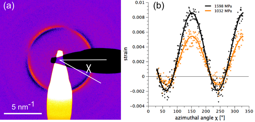
(a) Color coded image overlay of a distorted SAD pattern and its by 90° rotated and inverted counterpart. (b) Atomic level elastic strain (as a function of azimuthal angle χ) measured at two different stress states of the same sample position.
Amorphous thin films
Mechanical properties
Due to the lack of long-range order in amorphous structures the interrelation of the mechanical behaviour and the atomic structure is not easily amendable even for the case of elastic deformation. However, we demonstrated the applicability of atomic-level elastic strain measurements using electron scattering of micro/nanoscaled thin films in the transmission electron microscope by analyzing distorted selected area electron diffraction (SAD) images that can be acquired down to submicron scale [C. Ebner at al., Ultramicroscopy 2016; doi:10.1016/j.ultramic.2016.04.004].
In order to obtain the 2D atomic level strain tensor from the geometric changes of the first diffuse ring with sub-pixel accuracy an automatic evaluation procedure was developed. The corresponding Digital Micrograph Script can be downloaded from the Website. We are using this method to study in-situ in the TEM the structural and mechanical response of amorphous thin films deformed within the elastic regime. Hitherto, we focused on
- the elastic stress-strain response to calculate Young’s modulus and Poisson’s ratio,
- the local atomic-level elastic strain as a function of sample position (strain mapping),
- uncoupling anelastic and elastic strain and
- the time dependent anelastic and viscoelastic strain response.
Crystallization and atomic clusters
We are also interested to advance the fundamental understanding of both the structure and its stability of amorphous materials exposed to well-defined levels of irradiation or temperature. The investigations are based on aberration corrected in-situ (scanning) transmission electron microscopy ((S)TEM) of amorphous nanostructures ranging from thin films down to atomic clusters.
Nanocrystalline bulk materials
Nanostructured materials attract considerable scientific and technological interest since they exhibit new and enhanced physical and mechanical properties. In our group nanostructured materials are mainly processed by methods of severe plastic deformation (SPD) such as high pressure torsion and accumulative roll bonding applying deformations up to 100 000%. The focus of our research comprises fundamental aspects of grain refinement, defect evolution and phase stability of the SPD processed nanostructured materials. Bulk nanostructured metals, alloys and intermetallic compounds based on different long-range ordered structures are investigated. The materials are analysed by novel transmission electron microscopy (TEM) methods (like quantitative profile analysis of selected area electron diffraction PASAD) and on an atomic scale using high-resolution TEM. In addition, TEM in-situ methods (straining, heating and cooling) are applied. DSC is used to analyse various phase transformations. The TEM and DSC results are complemented by data obtained by X-ray and synchrotron scattering experiments.
Nanostructured thin films

Copyright C. Rentenberger
Nanostructured thin films
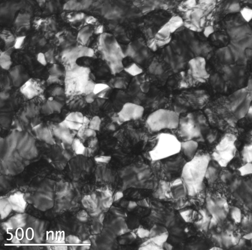
The deformation behavior of nanocrystalline metallic thin films is influenced by the dimensional constraints given by the grain size and the film thickness. In-situ TEM concomittant with stress-strain measurements is used to study the deformation processes of freestanding nanocrystalline thin films at different stages of deformation.
Image: TEM image of the defect structure of nanocrystalline Al thin film
