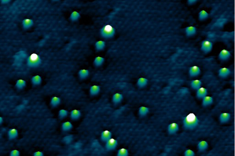
Graphene is a material made of a two-dimensional arrangement of carbon atoms, discovered in 2004, which has had a significant impact on the scientific community, leading to the awarding of the Nobel Prize in Physics to its discoverers in 2010.
The proposed method involves the controlled deposition of metal atoms, such as cobalt, during the formation of the graphene layer on a nickel surface. Some of these atoms are incorporated into the carbon network of graphene, creating a material with exceptional properties of robustness, reactivity, and stability even under critical conditions.
This new material can be detached from the substrate while maintaining its original structure and is therefore potentially usable in applications in catalysis, spintronics, and electronic devices.
The presented work is the result of an international collaboration between researchers from CNR - Istituto Officina dei Materiali, University of Trieste, University of Milano Bicocca, and University of Vienna.
Researchers' Comments
· Cristina Africh (CNR-IOM): "This is still a preliminary result, but already very promising, born from an original idea in our laboratory that initially seemed unfeasible".
· Giovanni Comelli (University of Trieste): "The contribution of diverse and complementary skills was crucial to demonstrate the effectiveness of this approach, which is both simple and powerful."
· Cristiana Di Valentin (University of Milano Bicocca): "We applied this method to trap nickel and cobalt atoms, but our calculations suggest that the use can be extended to other metals for different applications."
· Jani Kotakoski (University of Vienna): "We have shown that this material survives even under critical conditions, including the electrochemical environments used in fuel cells and batteries."
Published article V. Chesnyak, D. Perilli, M. Panighel, A. Namar, A. Markevich, T. An Bui, A. Ugolotti, A. Farooq, M. Stredansky, C. Kofler, C. Cepek, G. Comelli, J. Kotakoski, C. Di Valentin, C. Africh. Scalable bottom-up synthesis of Co-Ni-doped graphene. Science Advances 10, eado8956 (2024).
DOI: https://doi.org/10.1126/sciadv.ado895
Contact Information
Univ.-Prof. Dr. Jani Kotakoski
jani.kotakoski@univie.ac.at
+43-1-4277-72844
https://physnano.univie.ac.at/

