Equipment
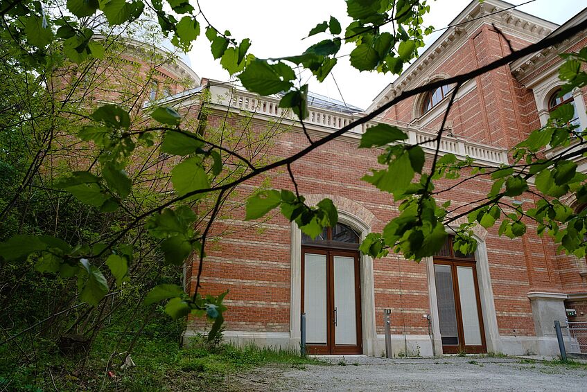
Physics of Nanostructured Materials (PNM) carries out research benefiting from state-of-the-art complementary experimental methods, such as atomic resolution scanning and transmission electron microscopy, transmission electron microscopy, associated spectroscopic techniques, and scattering with synchrotron radiation. The main instruments operated by the research unit are an aberration-corrected ultra-high vacuum scanning transmission electron microscope (Nion UltraSTEM 100) with versatile extensions for in-situ experiments and a Cs image-corrected transmission electron microscope (FEI Titan 80-300). Additionally, PNM also develops physical models to clarify the experimental results, and develops state-of-the-art computational techniques based on ab initio simulations. Most of the equipment is located in the 18th district of Vienna in the Universitätsternwarte, and old observatory building (how to get there).
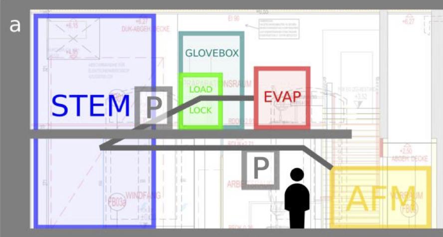
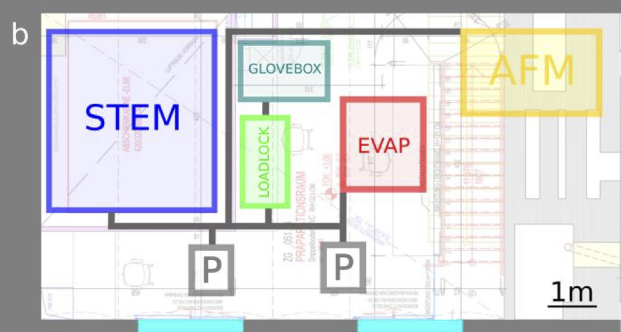
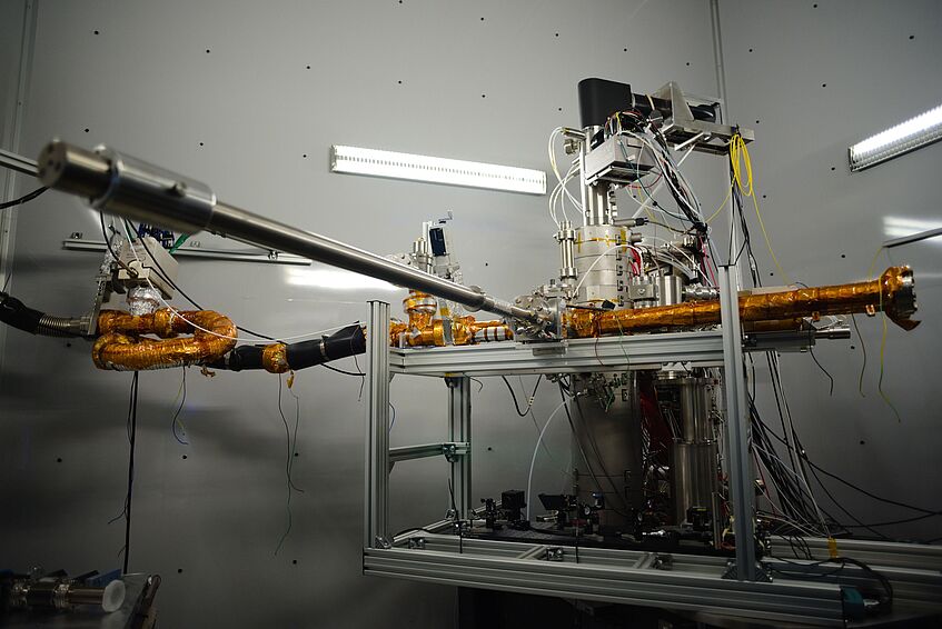
CANVAS (a system for Controlled Alteration of Nanomaterials in Vacuum down to the Atomic Scale) is built around an aberration-corrected ultra-high vacuum scanning transmission electron microscope, connecting several experimental stations in the same near-ultrahigh-vacuum. It allows preparation and growth of materials in a protective atmosphere (Ar glove box) and in vacuum (thermal and ebeam evaporators), their controlled manipulation (Specs plasma source), atomic force microscopy and mechanical testing (GeTEC AFSEM by Quantum Design), and atomic-resolution microscopy and spectroscopy (Nion UltraSTEM 100). The system is described in this publication.
Floorplan
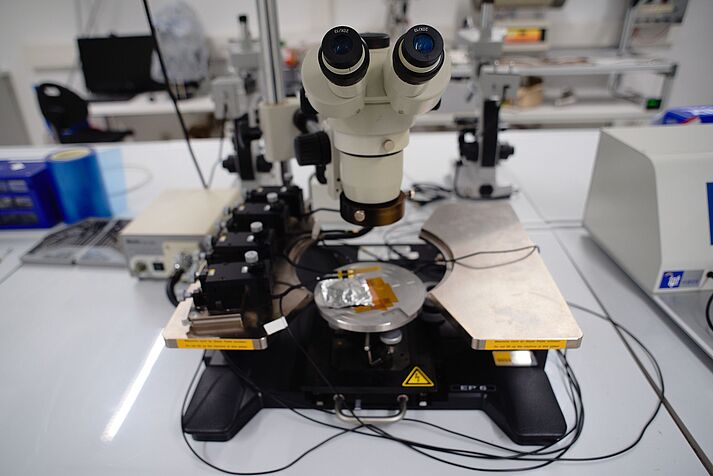
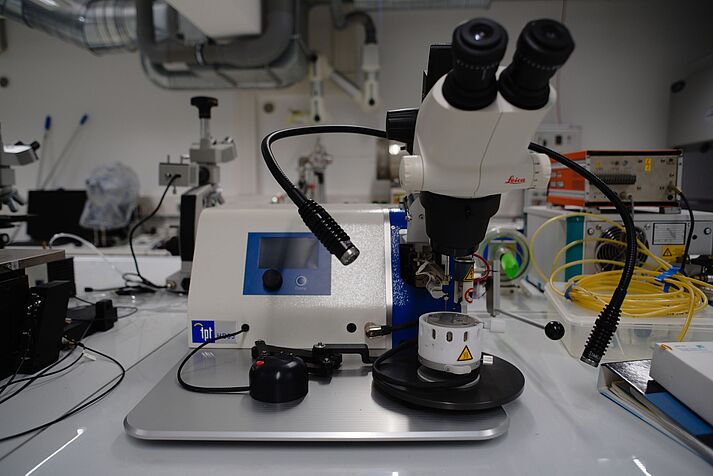
Sternwarte preparation laboratory is a basic chemical laboratory with equipment necessary for creating and precharacterizing 2D materials samples. The instrumentation includes a fume hood, chemical vapor deposition setup, Olympus BX51WI light microscope with a micromanipulator, small workbench for electronics, probe station, wire bonder, plasma cleaner and the low-voltage desktop electron microscope LVEM5.
Microscopes
The aberration-corrected ultra-high vacuum scanning transmission electron microscope Nion UltraSTEM 100 is at the heart of the group's experimental activities. The instrument has a constant-current operation mode for voltages between 55 and 100 kV with a probe size of ca. 1 Ångström, allowing atomic-resolution microscopy and spectroscopy. Its objective area has been modified for experiments in controlled atmospheres between 10-10 and 10-6 mbar, laser heating through a viewport, and an high-vacuum transfer line directly connecting it to the CANVAS system.
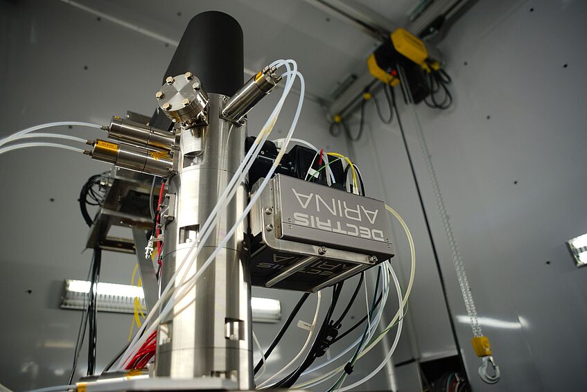
The Dectris ARINA is the latest-generation direct-electron camera that is optimized for ultrafast measurements at the lower primary beam energies. The Si-based sensor chip has 192×192 unusually large pixels of 100×100 μm in size, allowing it to accurately count every electron for any realistic electron-beam current. The speed of the camera is limited by the readout electronics' bandwidth of 10 Gb/s, resulting in a full-frame readout at 20 kHz or 2× binned and compressed readout at 120 kHz – corresponding to typical ADF scan rates. The ARINA thus enables uncompromising 4D-STEM measurements, bringing the group's experimental capabilities to the very leading edge of research worldwide.
For more information, see the Dectris website.
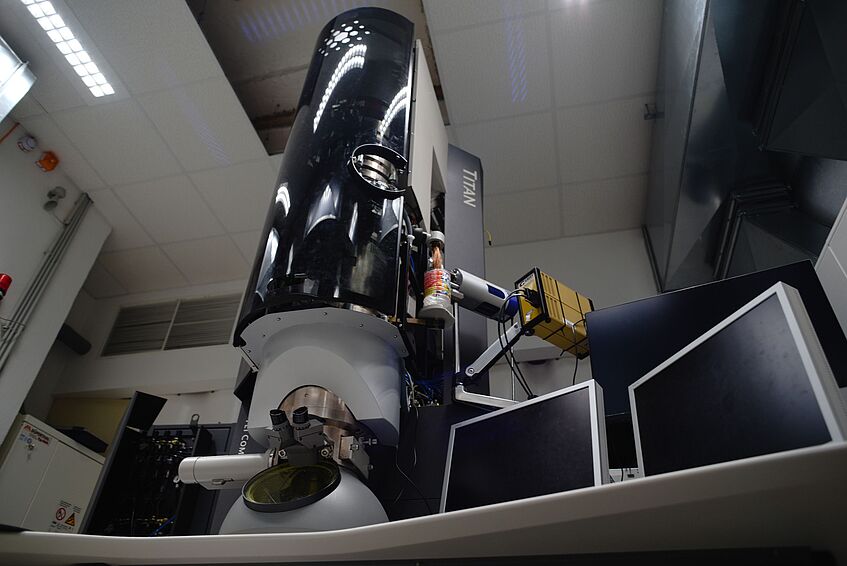
Transmission electron microscope from Thermo Fisher with an aberration corrector (CEOS Cs image corrector) an SFEG electron source, Gatan Tridiem 863 image filter for EELS, Oxford Instruments EDX system, and capabilities for tomography, scanning transmission electron microscopy, as well as liquid-phase and in-situ microscopy (mechanical, thermal and electric). Available acceleration voltages range from 80 to 300 kV (currently aligned at 80 kV, 200 kV, and 300 kV).
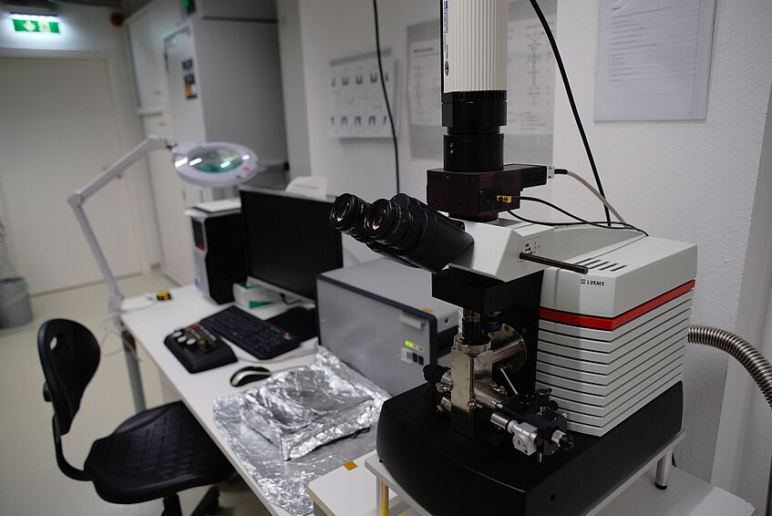
Delong Instruments Low-Voltage Electron Microscope (LVEM5) with an acceleration voltage of 5 kV. The microscope can be operated in transmission electron microscopy (TEM) and electron diffraction (ED) modes, as well as as an scanning electron microscope (SEM) and a scanning transmission electron microscope (STEM).
Other instrumentation
- High Pressure Torsion press type WAK-01 Mark 1, induction heating, cooling equipment, inert gas option, torque measurement
- Microhardness Indenter EMCOTEST DuraScan 20G5, HV0.05 - HV30
- Nanoindenter ASMEC Unat with QCSM module for depth dependent measurements and several indenters (Berkovich, Vickers, spherical)
- Universal mechanical testing machine SHIMADZU AG-10 TA AG-A R2 incl. Thermostatic Chamber (–180°C to 320°C)
- BOSE ElectroForce 3230 System III - mini-deformation machine for standard and fatigue testing up 300Hz and 450N
- Gas pycnometer Micromeritics Accupyc II 1350

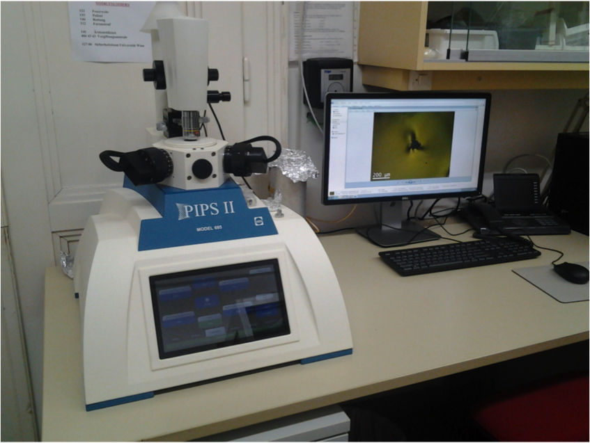
- Gatan PIPS II Ionmill with cooled specimen holder
- Spark-erosion
- Devices for electropolishing
- Grinding /polishing equipment
- Dimpler
- Stereo optical microscopes
- Differential Scanning Calorimeter PERKIN ELMER Diamond DSC
- Differential Scanning Calorimeter NETZSCH DSC 204 Phoenix
- Differential Scanning Calorimeter NETZSCH DSC/DTA 404PC/4/H
- Texture & Stress diffractometer AXS BRUKER D8 incl. VANTEC 500 area detector and polycapillary
- Profile Analysis (XPA) diffractometer with
- Rotating anode generator RIGAKU MM9 with monochromatisation Co-Kalpha
- Curved Position Sensitive Detector INEL CPS-590
- 4 Linear Position Sensitive Detectors (BRAUN, Photron-X)


